Microscopic Insight
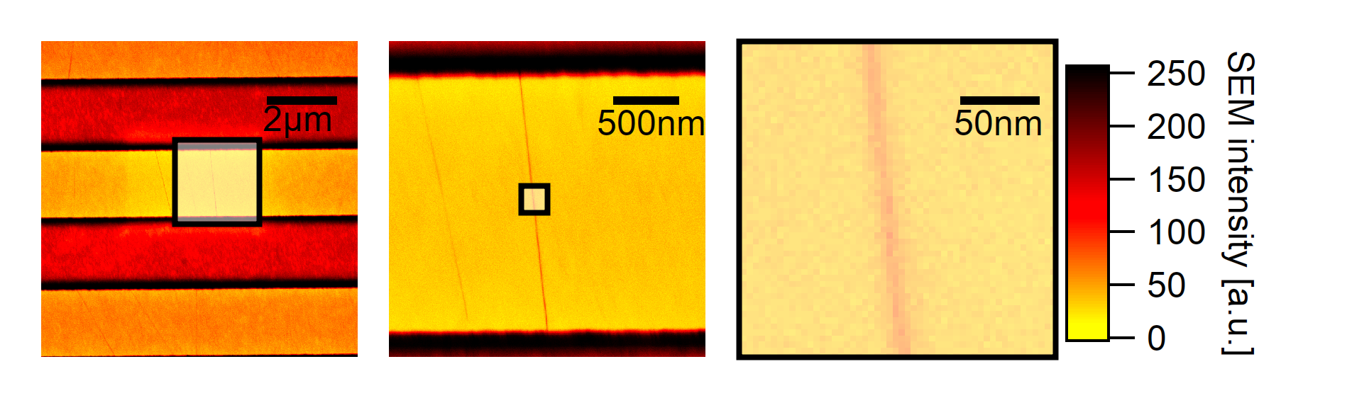
A carbon nanotube of 1nm diameter that is hanging over a trench structure of 2µm and is referred to as “freely suspended” in air.
Resolution Limit
The wavelength of the observed light limits the resolution in optical microscopy. Photoluminescence microscopy, therefore, has lower spatial resolution than electron microscopy, where the wavelength can easily be lowered by increasing the electron energy. Carbon Nanotubes typically emit light from the excitonic state at their first subband transition with a wavelength of around 1µm. Such SWIR emission limits the spacial resolution to about 500nm. However, the diameter of a nanotube is 1nm and around two orders of magnitude smaller. Photoluminescence microscopy may, therefore, not seem to be the first choice for analyzing nanoscaled systems.
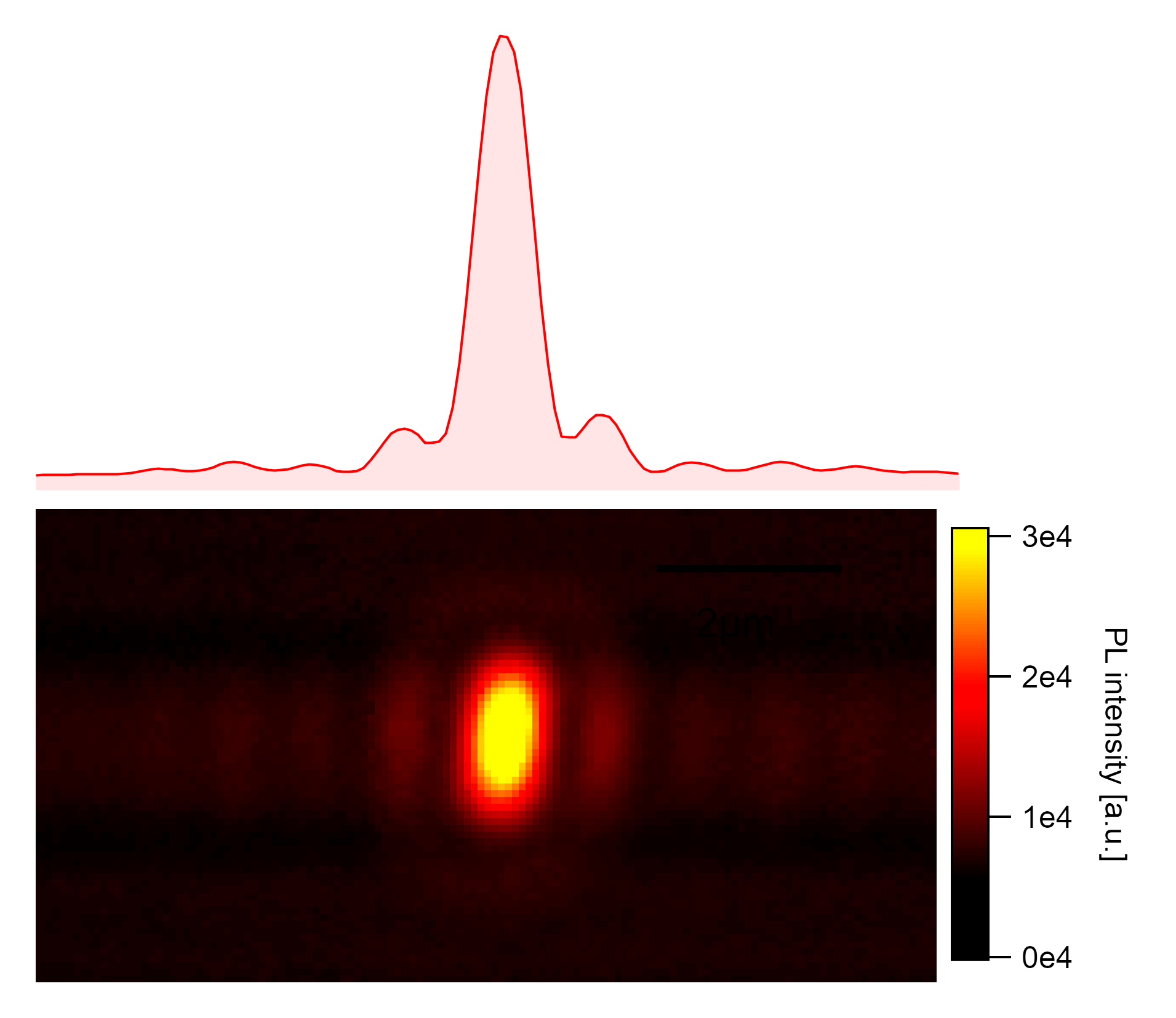
A typical SWNT hanging over a 2µm trench structure taken with high digital resolution. The luminescence is spacially broadened due to emission in the SWIR and shows phase information.
In the following chapter, I want to introduce the setup and recording technique for the microscopic setup that was devised to carry out all analyses in the following chapters. I also want to emphasize the insights that are possible from optical microscopy. This allows analyzing fundamental properties of the underlying excitonic particles like their diffusion length and their size by analyzing the phase information of images with high digital resolution (16bit).
Setup

Epifluorescence microscopy was performed on a Nikon Eclipse Ti series with an
Olympus LCPLN50XIR 50x near-infrared objective lens (NA 0.65). The objective
allows high working distances of up to 5mm and has superior transmittance of
around 70 to 90% in the measurement window between 830nm and
1300nm. The magnification in Nikon geometry is 83.3x with the built-in 1.5x
magnification enhancement of the Nikon microscope. The distance limits the
resolution for taking images with this objective to the first minimum of the
airy pattern:  This gives a maximally
resolvable distance between two point sources of around 0.75µm at emission
wavelengths above 800nm.
This gives a maximally
resolvable distance between two point sources of around 0.75µm at emission
wavelengths above 800nm.

The sample is placed into a glass cuvette that sits on a rotational and a nano stage.
The sample is mounted using a custom-built sample holder and placed into a quartz cuvette with a 1mm thick observation window. This allows flooding the measurement chamber with solvents. The cuvette sits on a Thorlabs PR01/M rotational stage and can be fine-positioned using a Physikalssche Instrumente (PI) P-563.3CD nano stage with 300µm positioning range in x, y, and z-direction using a PI E-712.3CD modular digital multi-channel piezo controller.
Cameras
Images in the near-infrared region (800-1000nm) were taken with an Andor Clara camera model DR-01374 with an integrated Sony ICX285 progressive scan silicon CCD image sensor with a square pixel size of 6.45µm and a 4:3 aspect of readable 1392x1040 pixels (1.5MP) which is an effective diagonal of 11mm on the chip. Thermoelectric cooling was set to hold -55℃, and the readout rate for images was 1Mhz, where the lowest readout noise can be achieved, and digitization of 14bit (without dynamic range) is possible. Images were saved both as 16bit unsigned integers using Wavemetrics Igor Pro binary wave and plain ASCII format. Quantum efficiency for the images in extended NIR mode is expected to linearly drop from around 30% at 830nm to 5% at 1000nm.
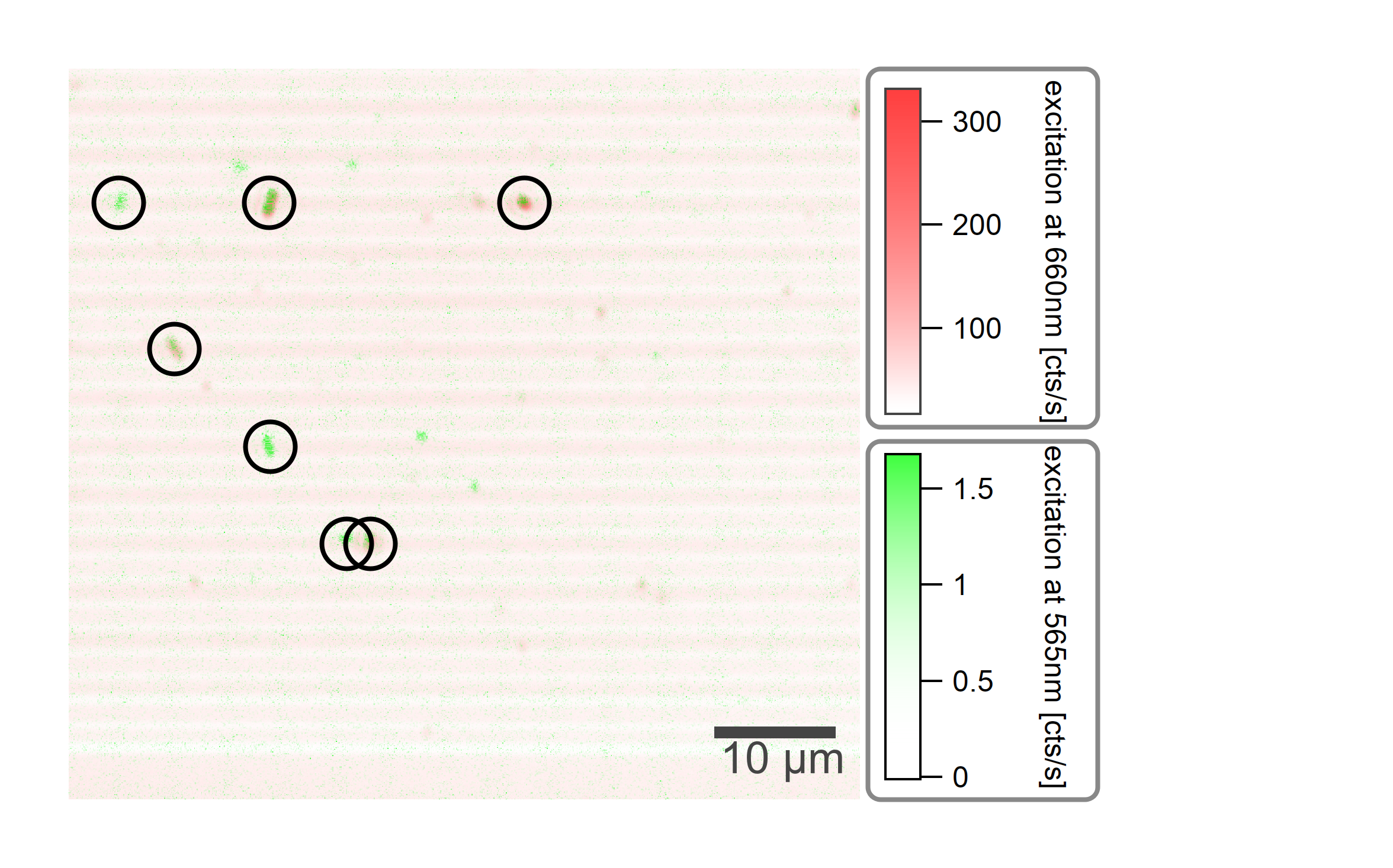
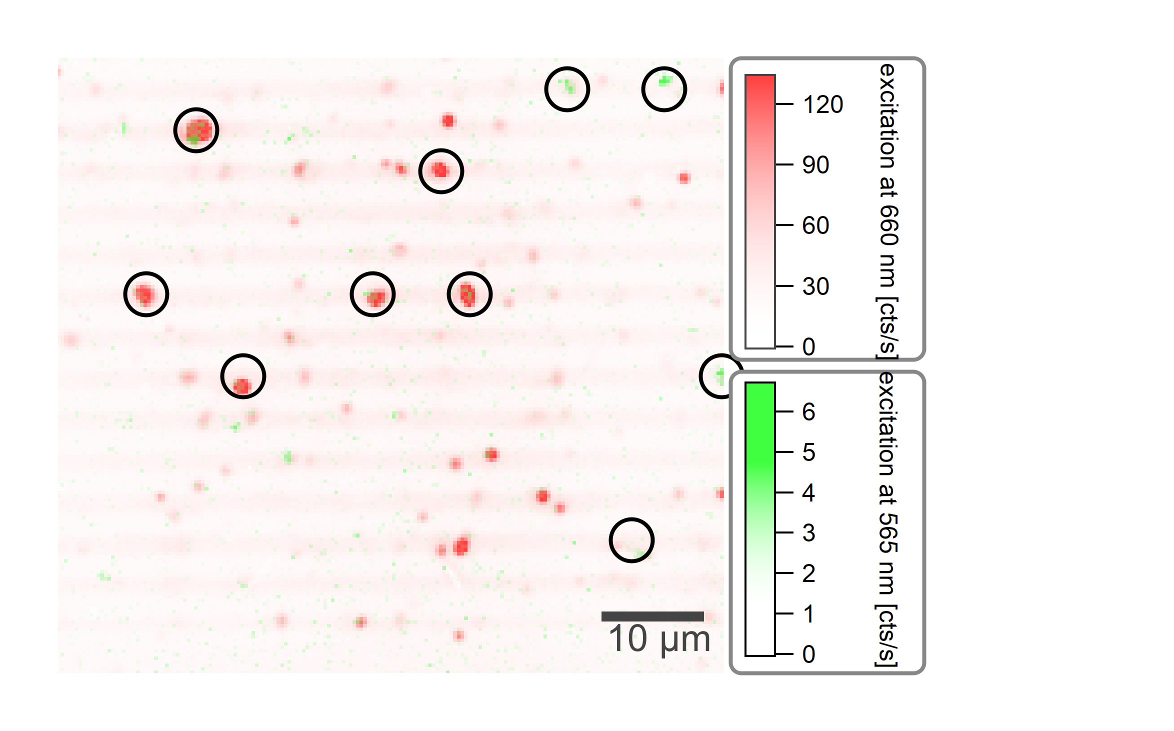
Andor Clara (Silicon) detector at different excitation wavelength marked with lime green (570nm) and deep red (660nm) color.
Even though the two excitations differ by a factor of 100 in power, the highest intensities differ by almost a factor of 200, which could be due to the low sample size of the nanotubes, excited by green light.
A Xenics Xeva-1.7-320 series with 320x256 InGaAs pixels (80kP) and a quadratic pixel pitch of 30µm was attached for image measurements in the short wave infrared (SWIR) region (0.95-1.25µm). The sensor’s effective array size is 12.3mm in diagonal, and illumination intensity is therefore nearly comparable between silicon and InGaAs camera. The camera is specified with a peak quantum efficiency of 80% and exhibits a near-linear photoresponse increase of 0.6 to 0.8A/W in the SWIR range with stable thermoelectric cooling at -70℃. It was specifically aligned for operation at 15s exposure times with high gain to achieve low readout noise. An unilluminated background image had always been taken and was subtracted to account for the high dark current.
The dark current of the InGaAs camera is 0.19·10⁶e⁻/s (specified at 280℃) which is around nine orders of magnitude higher than the 0.3·10⁻³e⁻/s of the silicon camera which dramatically influences the achievable image quality even though the quantum efficiency of InGaAs at 950nm is one order of magnitude higher than that of silicon. Notable is also that the dwell time significantly differs between the two cameras, and the InGaAs camera could not be operated at high exposure times (5min), which is needed for increased contrast in single-molecule spectroscopy.
Xenics Xeva (InGaAs) detector at different excitation wavelength marked with lime green (570nm) and deep red (660nm) color.
There is no significant benefit of the lime green excitation in the SWIR range as it only targets the (6,5) nanotubes.
Illumination
Images were illuminated using a Nikon TI-FL epi-fluorescence illuminator. The image area was illuminated with the iris of the TI-FL fully open. Images were taken using a 660nm dichroic mirror mounted to a Nikon microscopy cube assembly in the rotatable cube revolver of the eclipse. Two light sources were typically used: Thorlabs M660L4 for deep red illumination at 660nm and M565L3 with a 570nm bandpass for lime green. The sample was illuminated with a total power of 1.34mW for the red LED, and 350µW for the green LED (15µW with attached bandpass). The excitation intensity is nearly homogeneously (FWHM > 1mm) distributed over the illuminated camera area (0.1mm²). This low power excitation prevents the samples from being damaged by reaction with oxygen but also requires long illumination times.
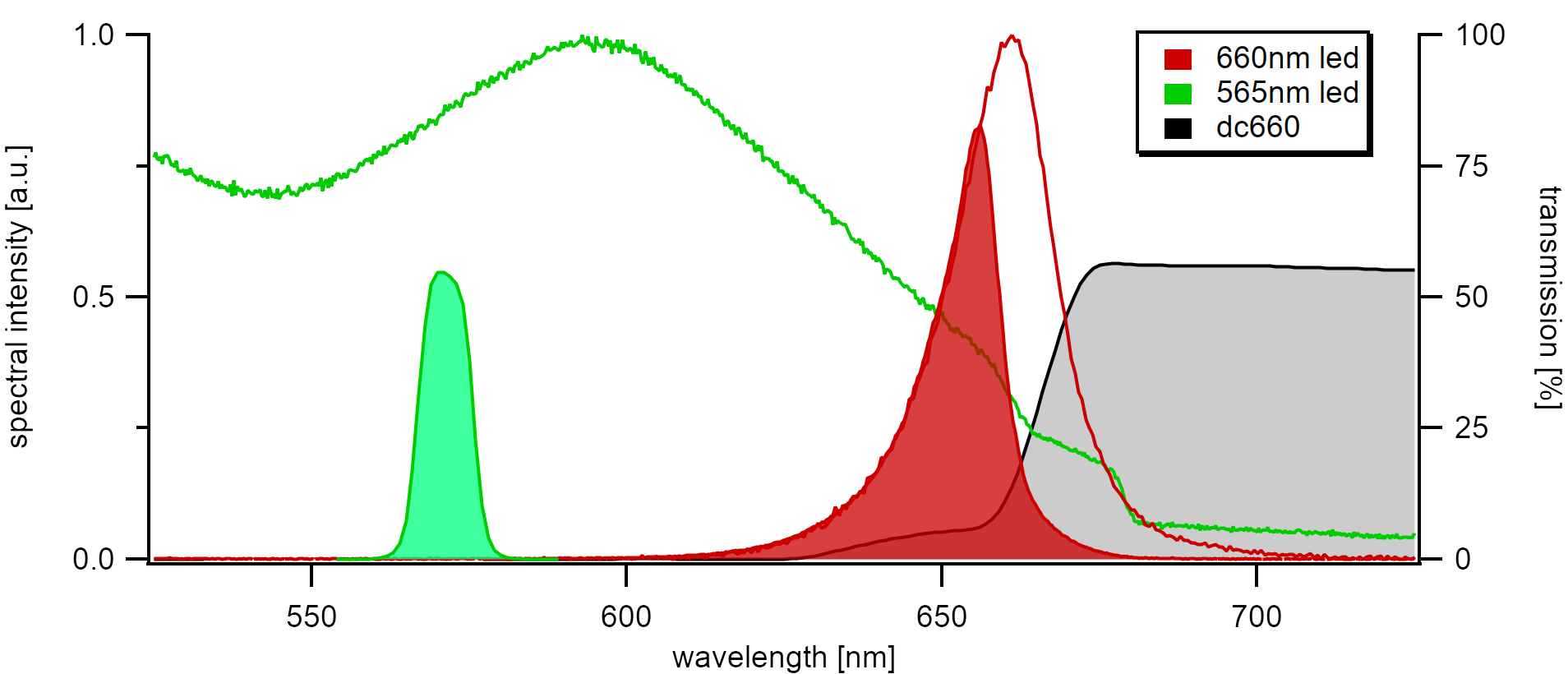
The figure shows the excitation spectrum of the deep red and lime green diodes. The red spectrum (660nm) is cut off at the edge of the dichroic mirror (dc660), and the green spectrum (565nm) is narrowed by a 570nm bandpass filter.
Data Acquisition
The measurements were performed using a custom build LabVIEW program and saved using Igor Pro binary waves (ibw). The measurement program allows automatic positioning with the nano stage and subsequent spectra recording for a set of coordinates. It also allows recording photoluminescence excitation maps and images in the same automatic manner. Data were further processed using Wavemetrics Igor Pro 8. Files were loaded using the PLEM loader and analyzed using typical automated tasks with the mass analysis package.
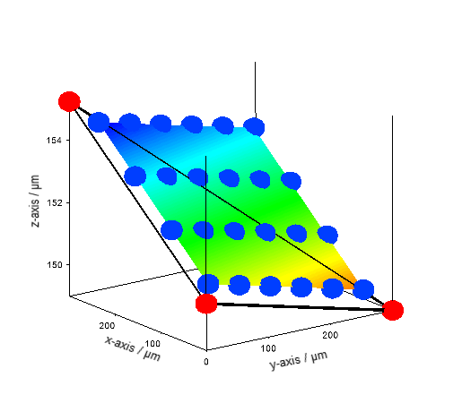
Calculation of the tilt plane for image acquisition and spectra recording.
The three points from SMAgetFocuspoints() are marked in red, and the
locations for image acquisition of the 300x300µm range of the nano stage
calculated from SMAcameraCoordinates() are marked in blue.
The sample tilt plane was measured using the 3-point technique described at Ishii et al.[136]. The maximum intensity of the laser reflection in the z-direction at 3 points on the sample surface was measured using the silicon camera and analyzed with SMAcameraGetTiltPlaneParameters() which generates the Hesse Normal form of the surface plane. From this, the exact z-position could be calculated. Best images are acquired when the laser focus is 2.5µm away from the sample surface with a rough tolerance of 1µm. Best spectra were measured when the laser was focussed on the surface.
The described technique allows detailed scanning of the image area that is only limited by the range of the nano stage. The acquired images also show that substantial background emission comes from the bottom of the trenches. This emission was found to disturb the recording of excitonic spectra as it increases in the SWIR. It could be reduced by accurately positioning the laser in the z-direction using the laser focus reflection from the sample plane as an offset to the calculated tilt plane parameters.
An overview of the available sample area (300µmx300µm) is constructed from 24 individual images at different focus positions recorded with the LED excitation centered at 660nm.
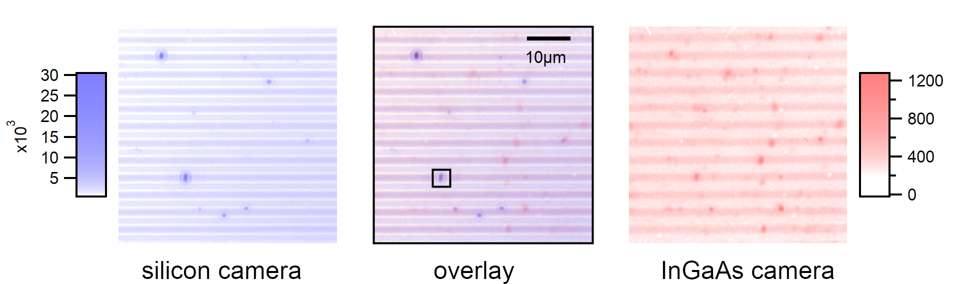
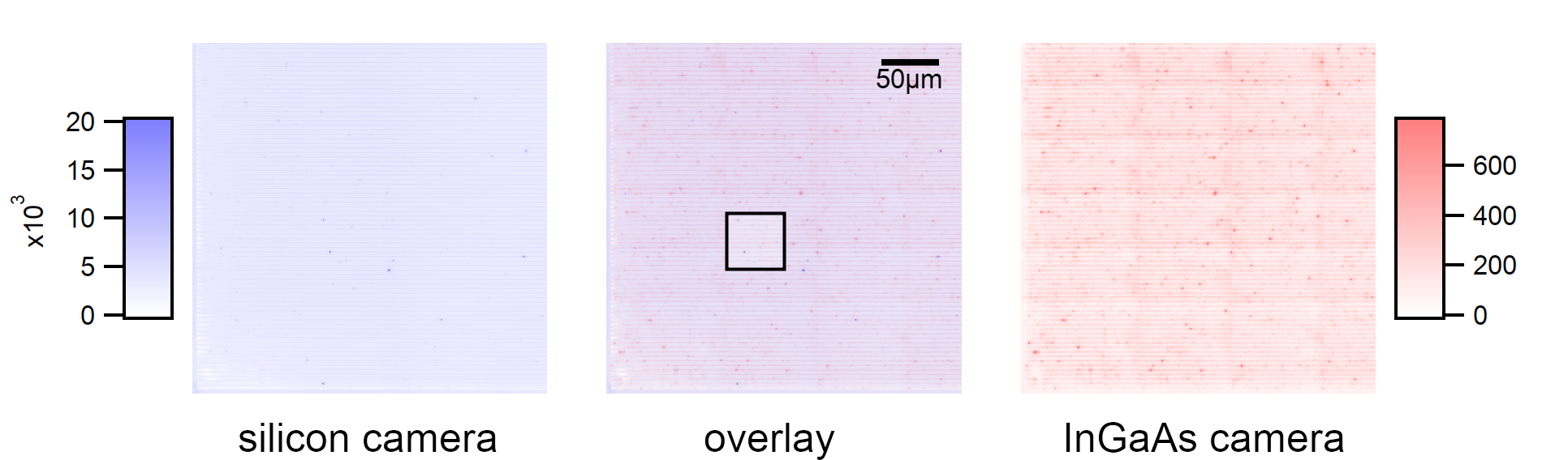
A comparison of the two cameras at different zoom levels shows that both cameras detect a subset of the available suspended nanotubes while some tubes (mostly (7,5)) are detectable by both cameras.
In all measurements except tilt plane measurements, an 830nm long-pass filter is attached to filter out the excitation spectrum.
Data Analysis
The acquired images show homogeneous photoluminescence along the nanotube axis and symmetrical rays around the nanotube. Homogeneous emission along the nanotube axis is typical for long nanotubes and is sometimes considered to originate from a highly fractured defect landscape that confines the emission to distinct unresolvable spots. [137] However, it is also reasonable that such homogeneous emission can also originate from perfect nanotubes leading to high diffusion lengths. Typical for the acquired images are the rays surrounding the central nanotube location, which are more prominent in the trench cavity parallel to the longitudinal extension of the suspended nanotubes. The images in this study exhibit an overly high digitization resolution compared to usually seen nanotube images [138][139], resulting in extremely high contrast. Images of lower digitization were recorded with the InGaAs camera but generally only show a blurred gaussian decay of the photoluminescence intensity perpendicular to the axis. The wide pixel pitch (and size) combined with the moderate numerical aperture of the objective lens used in this study does not allow to discover the presence of these bands with a typical InGaAs camera. The excellent full well depth of the Silicon camera at long illumination times allows studying these bands with exceptional digital resolution. In the following images, the false coloring is done on logarithmic scales to account for the exponential decay of the intensity in these bands. In the following, the origin of these rays is discussed to shed light on their origin. A simple optical simulation is included to substantiate estimations about the nanoscaled system that is responsible for these bands.
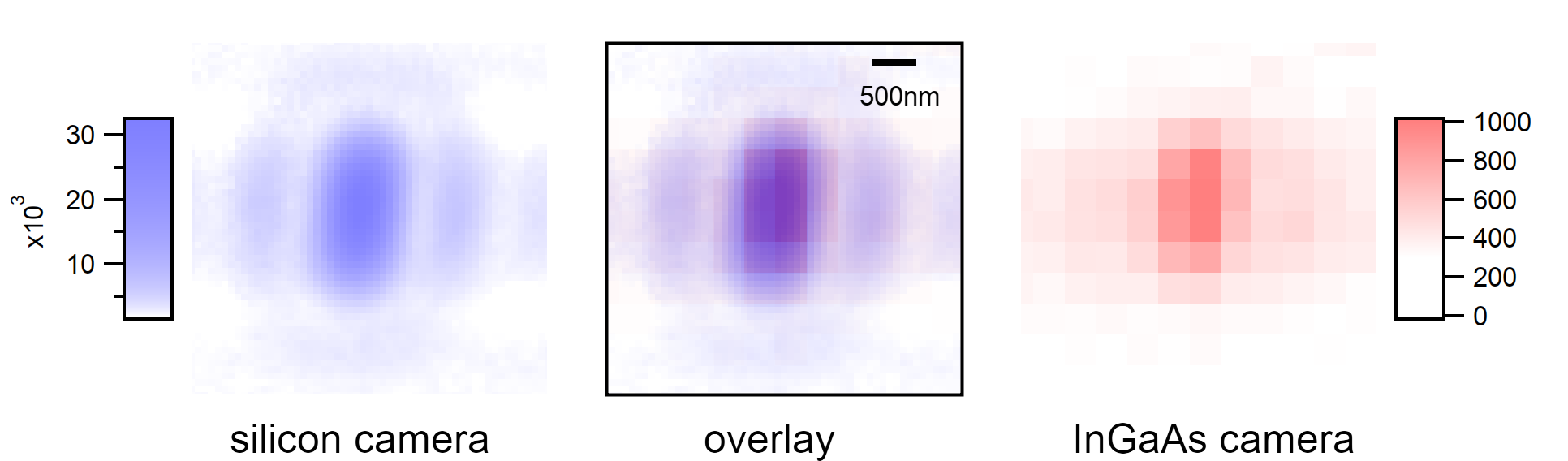
Two images taken from the same location with different cameras show the effective digitization difference between the two cameras. Left: Andor Clara (5min exposure), Right: Xencis Xeva (15s exposure)
The images are recorded with a 660nm led and an attached beam splitter at 660nm. The observed bands may originate from the superposition of Rayleigh scattered energies with the incident energy creating a standing wave. However, due to the attached dichroic mirror, direct Rayleigh scattering of the second subband transitions is not observable and is thus not considered here.
Due to its shape, the pattern must have its origin from the interferences of excitons emitted along the longitudinal axis. Reflections from the 3µm deep trenches are neglected as the emitted field E(θ) is expected to be homogeneous around the circumference. Such a homogeneous emission would lead to a decay of the radial intensity E(r) proportional to the (co-)tangent: E(r(θ)) = 2·3μm·tan(φ) with φ between 0 and π/2 for r→∞. However, the decay of the emission is rather exponential, extending far beyond a distance of 2µm.
Interferences caused by a reflection at the bottom of the trenches is also neglected since the led is considered a single photon emitter which allows assuming that only one exciton at a given time is emitted and excitons with different lifetimes that are emitted at different times are not probable to result in a large interference.
Simulation
To shed light on the origin of these side bands, a simulation of the images acquired with optical microscopy using Bessel’s functions for single exciton emissions is carried out. A Monte Carlo simulation is done to estimate the emission profile of excitons along the axis.
First Passage
For Exciton diffusion, the principle of fist passage is applied [140][141][136]. The rather complex mathematical approach is easily transferred to the following simulation:
Excitons are allowed to diffuse freely along the tube axis. As soon as they hit a quenching site, they are blocked from further diffusion and decay non-radiatively. Quenching sites in this simulation are the ends of the nanotube that touch the silicon wafer surface. The nanotubes are considered defect-free without adsorbed molecules.
Excitons are generated using a homogeneous probability along the axis originating from the illumination with a spatially homogeneous light source. In this example, the (6,5) type is taken for the simulation, which emits from its first excitonic subband at a wavelength λ of 930nm.
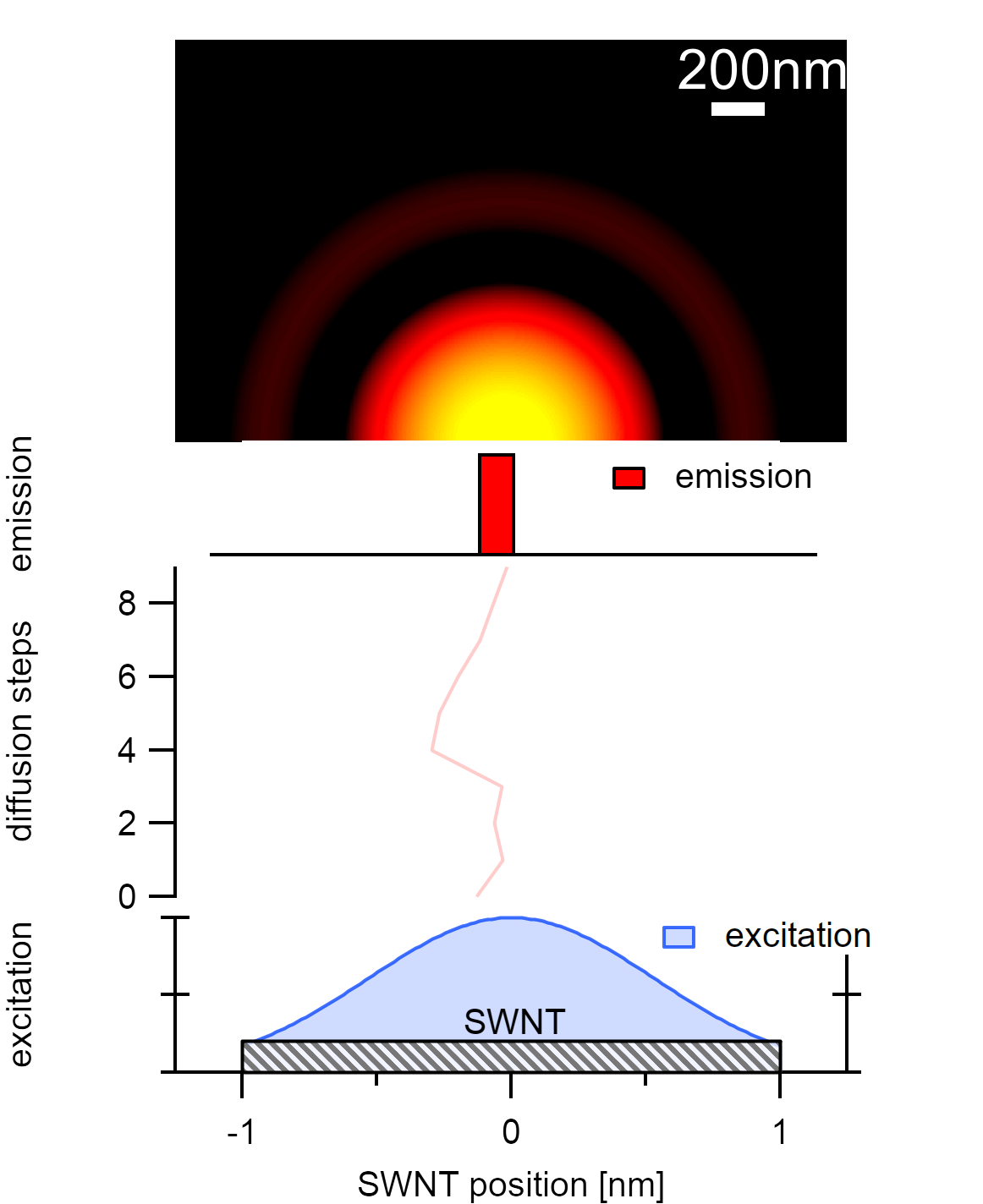
An exciton is generated in the center of the nanotube by a gaussian shaped laser profile. The exciton diffuses over nine steps and decays radiatively, which gives the (axially symmetric) point spread function of single excitonic emission calculated for one lateral side.
The emission aperture is approximated with the longitudinal exciton diameter a and the observer distance d is set equal to the working distance of the objective (5mm), neglecting a 1mm thick quartz glass window between observer and nanotube at a distance of 1mm from the silicon wafer surface. The point spread function PSF(r,θ) for the emission is approximated with an airy disc of diameter a in cylindric coordinates using Bessel’s function of first-order J₁ from the SLATEC Common Mathematical Library as a solution to diffraction-limited beams:

The LED is operated at low power densities and has considerable temporal coherence in the 10ms range to only excite one exciton at a time. This makes it reasonable to neglect electronic many-body effects like exciton-exciton annihilation and phase space filling for the simulation of these images.
Note
The assumption that only one exciton is generated at a time is based on the relative absorption cross-section of 1.710⁻¹⁷cm² per carbon atom [142][143]. This is used together with the central emission wavelength of 660nm at irradiation of 1.5W/cm² to estimate the generation of excitons in this system to 85 excitons per carbon atom and second. For the (6,5) type, which has 88 carbon atoms per nm [144], this gives 15 million excitons per second on a 2µm long carbon nanotube. As the generated excitons have an estimated decay time of less than 350ps, this allows assuming that only one exciton at a time is generated in the system.
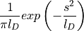
In comparison to laser excitation, however, quenching at the ends of the nanotube tips or respectively at the contact to the silicon substrate can not be neglected. The irradiation with a laser was simulated and compared to homogeneous irradiation. While the images from laser irradiation show emission from the center of the nanotube similar to a point source, the emission from homogeneous excitation show wider spreading along the nanotube axis with a bone-like emission profile.
Exciton Diffusion
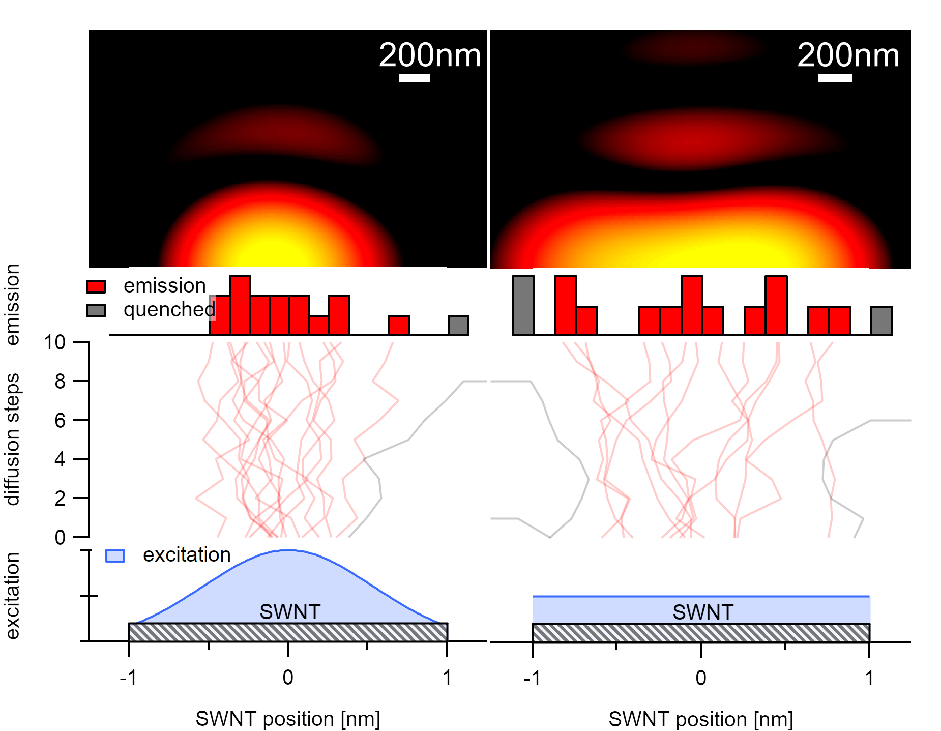
The emission profiles of two 2µm long carbon nanotubes illuminated with a light source of spacially homogeneous intensity (left), and a gaussian shaped profile (right) show that end quenching effects and diffusion length are not neglectable in this system.
For a typical simulation, 2048 excitons are allowed to decay after 10k diffusion steps radiatively. They emit from spots on a 24nm spaced potential energy landscape [145]. The length of the nanotube is fixated in the simulation at 2µm neglecting elongations caused by nanotubes dispersed non-perpendicularly.
Due to end quenching effects, the spatial emission profile upon homogeneous
emission is primarily governed by the exciton diffusion length. Within the
simulation, the diffusion length was varied. For a typical image, 10k
diffusion steps are calculated while the diffusion length  is
distributed with a Gaussian probability to give the displacement s
[136].
is
distributed with a Gaussian probability to give the displacement s
[136].
Discrete diffusion steps are necessary for the model of first passage to
eliminate excitons that hit a quenching site during their lifetime. Due to
Fick’s law, the quadratic diffusion length is proportional to the lifetime
 . This readily gives the diffusion length
 for N diffusion steps at a fraction N of the lifetime τ:

The diffusion length is typically estimated to be 10nm for short-lived excitons [146] and 100nm [147][148] up to 1 micrometer [141] for the long-lived excitons that are relevant for photoluminescence. Within the simulation, the diffusion length is varied between 10 and 1000nm, which allows simulating the effects on the squared combination of all PSFs. In the simulated diffusion range, the emission intensity shape at the tips of the nanotubes varies. These end quenching effects allow estimating that the diffusion lengths in these samples are greater than 350nm but could also be up to 1µm. It has to be noted, however, that as the diffusion length approaches the nanotube length, a significant amount of excitons is affected by end quenching. At diffusion lengths of 1µm, this typically affects 75% of the excitons in a 2µm long nanotube. The amount is reduced at lower diffusion lengths. While at 350nm, 30% of the excitons decay non-radiative, at 100nm 8%, and at 10nm, only 0.5% are affected by end quenching.
The exciton diffusion length determines the shape of the excitonic emission. At low diffusion lengths (<100nm), end quenching becomes neglectable (left) while at diffusion length above 350nm, it is significantly high, and the shape loses its bone-like structure (right).
Relying on the results of this simulation, we estimate end quenching effects as the dominating decay process in suspended nanotubes that are homogeneously excited at low fluence. This finding is especially important for nanotubes shorter than 2µm, where the nanotube length approaches twice the diffusion length. A reduction in diffusion length can, therefore, yield brighter photoluminescence even in air, which was already shown for quasi-zero dimensional systems with excitons immobilized at oxygen defects [149].
Exciton Size
The exciton size a can be approximated from the phase information of the transverse radial part of the observed airy discs. A commonly used size of 2nm was measured using SC-dispersed nanotubes [146]. Newer studies suggest that this size is by at least a factor of 6 higher for better-individualized nanotubes [150][144]. For a suspended (6,5) type, which was taken as a reference for the simulation, the exciton size is estimated to be 8.5(5)nm. This is by a factor of 3-4 larger than most estimations but also by a factor of 2 lower than the recent approximations for nanotubes with a strong dielectric screening [144]. In environments with low dielectric screening as in air-suspended nanotubes binding energies of around 725meV [151] are found, which is by a factor of 2 higher than in micelle encapsulated nanotubes [39]. An exciton can be approximated with a hydrogen atom where the radius is inverse proportional to the energy. Double the energy gives half the radius, which makes an exciton size of 8.5(5)nm reasonable compared to the size of 14(3)nm at half the binding energy.
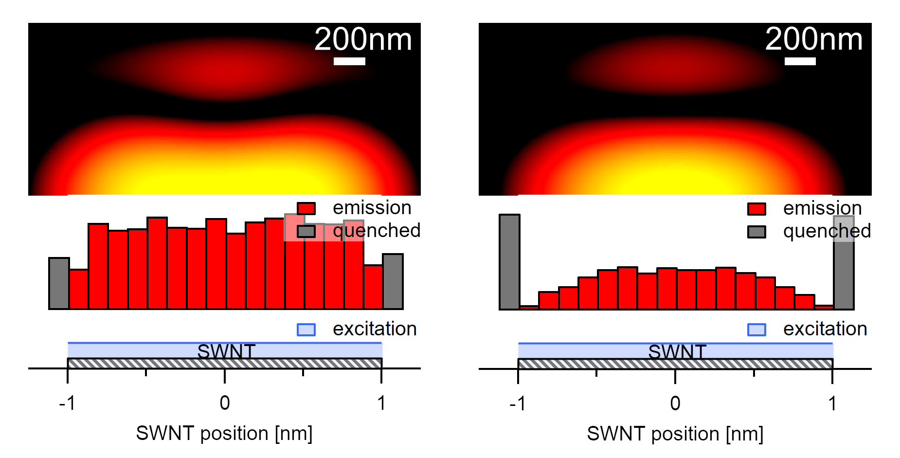
The simulated airy disc pattern shows good agreement with the camera images at a simulated emission aperture of 6.5nm.
A simple airy disc for the excitonic emission is only a rough approximation. The circular aperture is not a good approximation of an exciton considering the reasonably large exciton sizes. The aperture should rather be elliptically shaped, which would influence the above approximation for end quenchings. The fact that the airy disc is not perfect can also be seen from the comparison of the intensity in the first and third horizontal maximum of the measured and calculated images. For a more exact approach, a linear combination of higher-order Bessel functions has to be used, which leads to more complex solutions to the Fraunhofer diffraction equation.
Far Field Propagation
The easiest of these solution is a monochromatic wave propagating in z direction with a phase factor that describes the pattern in the (x,y) plane. It is conveniently described in cylindric coordinates [152]:

The radial and transverse wave vector along z satisfying
 and the radial coordinate in
the (x,y) plane
and the radial coordinate in
the (x,y) plane  . Bessel’s functions generate the periodic
part of the airy pattern. The phase factor, though, is invariant to the
distance from the source. Such waves extend with a slow exponential decay
along the z-axis, and their radial intensity profile in the (x,y) plane is
independent of the distance z. The first order beams carry phase information
and are thus able to reconstruct in the far-field [153].
Non-diffracting Bessel waves have been found as special solutions to the
Helmholtz equation [154] if the radius of the emission source is
far smaller than the wavelength of the emitted light. This is the case for
carbon nanotubes as they emit at wavelengths of around 1µm with exciton sizes
smaller than 10nm and a potential energy landscape of 24nm.
. Bessel’s functions generate the periodic
part of the airy pattern. The phase factor, though, is invariant to the
distance from the source. Such waves extend with a slow exponential decay
along the z-axis, and their radial intensity profile in the (x,y) plane is
independent of the distance z. The first order beams carry phase information
and are thus able to reconstruct in the far-field [153].
Non-diffracting Bessel waves have been found as special solutions to the
Helmholtz equation [154] if the radius of the emission source is
far smaller than the wavelength of the emitted light. This is the case for
carbon nanotubes as they emit at wavelengths of around 1µm with exciton sizes
smaller than 10nm and a potential energy landscape of 24nm.
Without making assumptions about the shape of the generating PSF, the observed
wave function  can be destructed into its spacial
autocorrelations using Fourier Analysis or a Wigner quasi-probability
distribution. The Wigner distribution
can be destructed into its spacial
autocorrelations using Fourier Analysis or a Wigner quasi-probability
distribution. The Wigner distribution  disassembles the wave function
from real space into phase space, allows to visualize phase information, and is
thus able to emphasize the source of interferences in the camera images.
disassembles the wave function
from real space into phase space, allows to visualize phase information, and is
thus able to emphasize the source of interferences in the camera images.
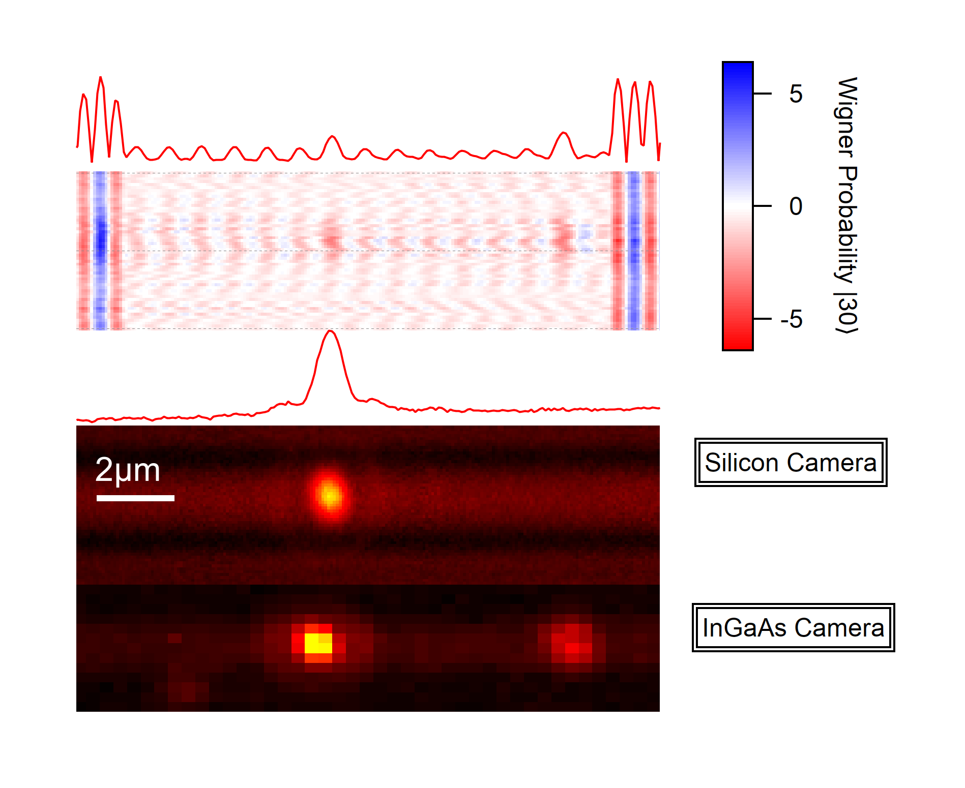
An astonishing feature of non-diffracting Bessel waves is that they are able to reconstruct in the far-field. This allows detecting asymmetries in the electric far-field, making SWIR nanotubes visible for the silicon camera.
Such a reconstruction of the generating wave functions using Wigner Transformation is able to reveal far-field interference of nanotubes. The surprising outcome of this interference is that nanotubes that are usually only visible with the InGaAs camera can be detected if they are located in the surrounding (~6µm) of a Silicon-active nanotube. This far-field interaction confirms the presence of non-diffracting Bessel waves emitting diffraction-free. The datasets need more sophisticated analysis to study if this interference is wavelength-independent as the phase factor suggests and up to which distance it is able to reconstruct the phase.
Conclusion
Microscopy images of carbon nanotubes are recorded at the optical resolution limit. From the shape of these images, it is possible to estimate an exciton diffusion length higher than 350nm in 2µm long carbon nanotubes. Images recorded with high digital resolution reveal the phase of the emitting point sources. This phase holds information about the wavelength and size of the emitter. As the wavelength was also measured, it is possible to estimate the exciton size to 8.5(5)nm. Emitting sources where the emitter size is much smaller than the emission wavelength are able to reconstruct in the far-field. This allows detecting the source of excitonic emission interferences by analyzing the phase information making excitonic emission visible solely by their phase and independent of their emission energy.